On the latest EE Times Europe Magazine (February 2021), our CEO, Chouki Aktouf shared his vision on how EDA methods and tools should change to conquer new SoC Design challenges.
SoC design starts with the integration process, in which the selected intellectual-property blocks must be interconnected. The challenge is reaching the best possible power, performance, and area (PPA) combination within tight deadlines while keeping engineering costs under control. In the traditional EDA design flow, each task — power consumption, architecture, testing, and so on — is performed separately by an ultra-specialized team of engineers, and achieving the completed design requires close communications and continual information exchange among the disparate teams. Each new iteration of a design restarts the information exchange process. As a result, the higher the number of iterations, the greater the impact on the project’s final cost and time to completion.
One reason that the traditional SoC integration flow inevitably generates many iterations is register-transfer–level (RTL) design, which needs to be fine-tuned and incrementally optimized until the RTL2GDS synthesis process reaches the best PPA result. Also, design reuse of soft IP cores from previous projects needs to increase to much higher ratios in order to extract more value from designs and to make IP cores and SoCs off-the-shelf commodities. Finally, cutting-edge change in design methodologies — representing a radical departure from traditional EDA practices and tools — must occur to accomplish the higher number of tasks that today’s SoC projects require without stretching engineering resources too thin. It is worth noting that most of the EDA innovations are expected to happen at the architectural level, during the SoC integration and before RTL2GDS implementation.
The methodology changes described below will help overcome the challenges.
1 - Start the SoC Build process much earlier
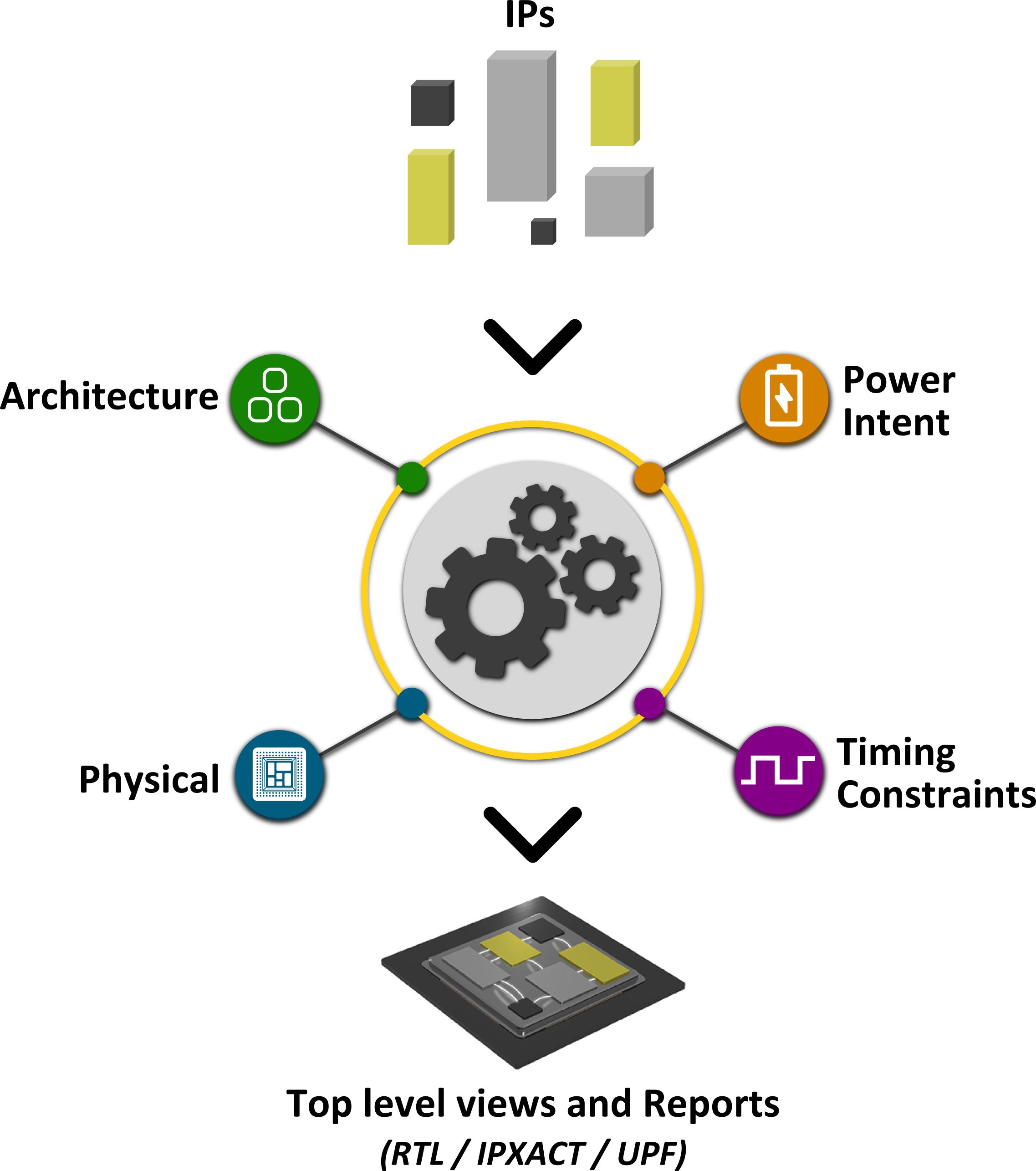
Accelerating this process requires that EDA design tools provide a much higher degree of automation when handling design information. The solution is a unified database that accommodates a variety of design domains and formats. All design information, including RTL, timing constraints, power, physical, and test, must be taken into consideration as early as possible in the SoC build process.
Such an approach, in practice, should allow non-domain experts to make important design decisions. For example, a CAD engineer or RTL designer would have the capability to build a first SoC configuration from design assembly to synthesis.
2 - Maximize Design Reuse ratio
Substantial resources are expended when building configurable IP subsystems for complex SoCs. Lowering the overall cost of SoC design therefore requires a much higher IP-reuse ratio than has traditionally been the case, and meeting that challenge requires a new class of design reuse methodologies and tools. During the SoC integration process, EDA tools must provide generic APIs with basic and advanced design extraction capabilities.
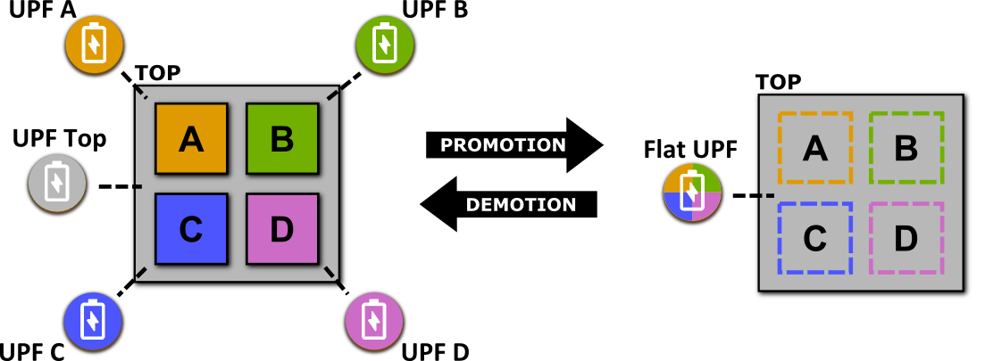
Let’s consider the example of an SoC integration requirement for a low-power application. The power architecture or intent is captured in a Unified Power Format (UPF) database. Before assembling or promoting power information at the SoC level, power information for the different blocks is extracted. Traditionally, power extraction has been a tedious, manual process. UPF demotion, however, is increasingly a process that requires full automation.
3 - Facilitate Design-Space Exploration
Another shortcoming of traditional SoC integration approaches is insufficient automation of the process for exploring the design space and determining the best PPA design configuration. The amount of engineering resources required to run multiple what-if scenarios manually may be excessive, preventing design teams from achieving optimized solutions.
Equipped with the physical design information, EDA tools should enable physically aware SoC assembly by creating different design configurations at the register-transfer level. This allows RTL detection and correction of problems that designers would otherwise discover only after synthesis. Such issues include connectivity problems, which can make placement and routing (P&R) a painful process.
4 - Make EDA tools smarter
Applications are expanding for AI and its derivatives, particularly machine learning (ML). The EDA community cannot neglect the opportunity to leverage ML algorithms when to resolve SoC design challenges.
