- Details
Defacto Technologies wants to simplify the design of electronic circuits
Based in Grenoble, France, Defacto Technologies markets software tools for creating complex integrated circuits. In 2024, Defacto has been named winner of the European EIC Accelerator program and will receive 2.5 million euros in grants to develop its new technological solution.
Simplify the task of designers of complex electronic circuits. This is the promise of the company Defacto Technologies, based in Grenoble and specialized in the development of software for the microelectronics industry.
Defacto has been named winner of the EIC Accelerator program, dedicated to supporting innovative European SMEs. In this context, the company will receive a grant of 2.5 million euros to launch an innovative software solution. In addition to this financing, the SME must invest more than one million euros of its own funds and take out some loans to complete, at nearly 4.1 million euros, the overall envelope necessary for this project, running on two years. “This amount will mainly be used for job creation, because we need to expand the team in terms of expertise,” explains Chouki Aktouf, president of the company, which he founded in 2003. Around ten hires are planned, an almost doubling of the workforce of this company which currently has 12 people at its headquarters in Isère and one employee in Palo Alto, for its Californian subsidiary. “Automate as much as possible” Marketing is planned for the second half of 2026. “It will be a new generation of software which will offer a global solution,” assures the CEO.
In the microelectronics segment, the design software market (EDA for “Electronic Design Automation”) is worth $9 billion globally. Defacto evolves in the more restricted niche of so-called “front-end” software: these cover the first stages of design, where the different electronic functions are intertwined, as opposed to “back-end” tools, closer to the physical manufacturing processes of electronic chips.
For the creation of complex integrated circuits, the assembly of pre-designed bricks represents a key step. “It’s a bit like Lego, with hundreds of blocks to connect together,” illustrates Chouki Aktouf. “Except that as the complexity of circuits increases, we want to automate as much as possible in order to have a simple and easy solution. » 30% time saving.
This automation will be based on internal technologies from Defacto Technologies and on “artificial intelligence”. More concretely, the software will rely on libraries to automatically create integrated subsystems, thus reducing design effort: “Instead of managing a thousand blocks, the designer will only see around thirty », explains the manager, estimating the time saving of 30%, compared to traditional tools.
This project has been funded by European Union.

- Details
The Automated SoC Design from Specification and Exploration to RTL Generation by Achieving Cost-effectiveness and Sustainability
With the miniaturization of components, transistor density is increasing faster than the productivity of system-on-chip designers and the improvement of EDA tools. Therefore, the SoC Planner Project aims to provide system-on-chip designers with a solution to the explosion in design costs, particularly for advanced nodes.
This project intends to develop an innovative and indispensable reference software suite for all hardware designers, enabling automatic configuration and planning of the next generation of system-on-chips, guaranteeing the best compromise regarding cost, performance, and eco-design criteria.
The main novelty of the SoC Planner project is to limit the number of possible configurations for a complex system-on-chip from the very start of a new design project. It is usual to have hundreds of thousands or even millions of possible configurations for a single project.
SoC Planner innovation will drastically reduce this number to a set of relevant configurations in line with the scope of the designer specifications at early stages. This will significantly reduce the number of design cycles (iterations of the product development) and, consequently, development cost savings. An eco-design dimension is also taken into account to enable precise measurement of environmental impact at the start of a new system-on-chip design project, and the minimization of this criterion in the same way as the usual performance criteria (consumption, time, surface area).
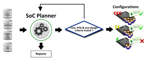
SoC Planner addresses sustainability at the early stages of SoC design by integrating eco-friendly principles throughout every step of the design process. SoC Planner combines the strength of several tools from CEA, Defacto Technologies and Innova Advanced Technologies. Through a user-friendly graphical interface, SoC Planner automates the exploration and optimization of computing architecture designs to find the most suitable configurations and generate the related SoC RTL design automatically.
This project was funded by BPI France as part of the France 2030 program.
![]()
